Choosing the right printed circuit board affects every stage of a product, from early prototypes to stable production. A Double Sided Pcb offers conductive copper layers on both sides, allowing designers to place more components without greatly increasing board size. This structure can support compact control panels, sensor modules, lighting systems, and industrial equipment. It creates useful routing space. That matters.
In practical projects, engineers often select this board when a single-sided layout becomes crowded. Through-hole vias can connect traces between the two copper layers, while careful component placement helps shorten signal paths. Better routing may reduce wiring complexity and improve assembly consistency. However, a double-sided design is not automatically superior. It may require more careful inspection, soldering control, and thermal planning. Poor via placement can still create bottlenecks. More copper does not fix weak engineering.
Reliable results depend on more than board thickness or layer count. Material selection, copper weight, surface finish, trace width, clearance, and operating temperature all deserve review. Experienced manufacturers also check fabrication tolerances before finalizing the layout. That step can prevent unexpected rework. Yet real projects rarely follow the first plan perfectly. A prototype may reveal uneven heat, difficult testing access, or traces that are too close for comfortable production. Those findings should guide revision, not be hidden.
This article examines why a Double Sided Pcb may suit your next project. It considers design flexibility, electrical performance, manufacturing demands, cost, and long-term reliability. The goal is practical judgment, not a universal recommendation. Sometimes, a simpler board remains the better choice.
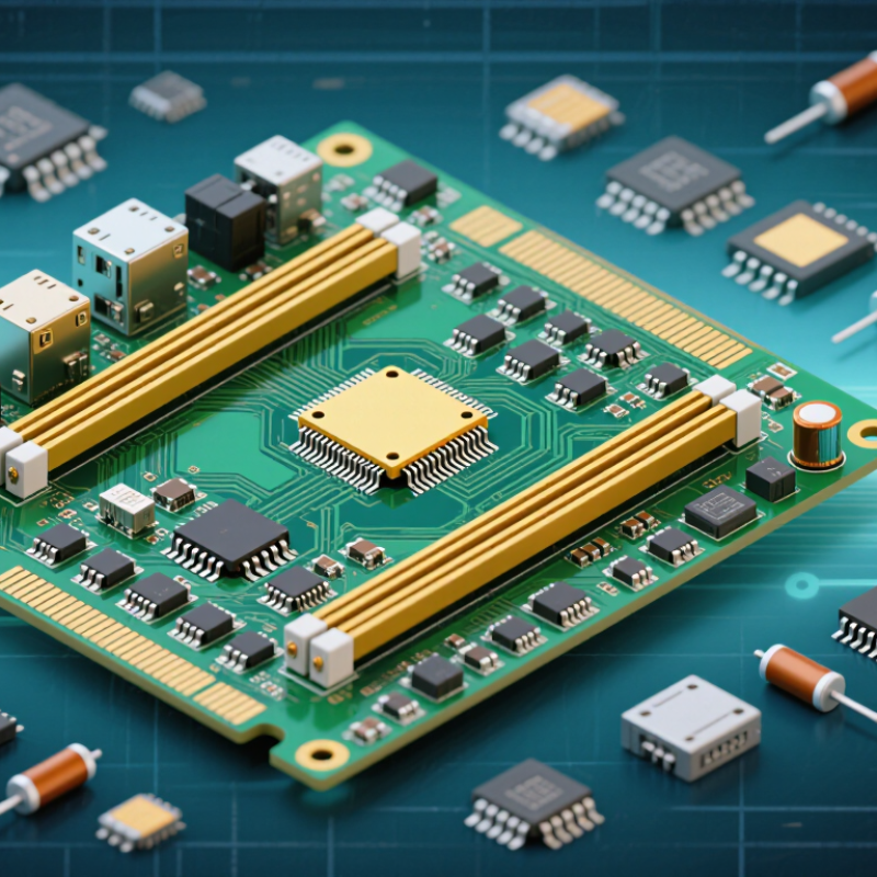
A double-sided PCB carries copper tracks on both its top and bottom surfaces. Plated through-holes connect these layers electrically and mechanically. Small vias let signals move between them without adding external wires. Components may sit on either side, which saves valuable board space. The result is compact. That detail matters in controllers, sensors, and power modules with limited enclosures.
During operation, one layer can route signals while the other supports ground, power, or additional connections. Designers must control trace width, spacing, and current capacity carefully. A short, direct return path can reduce noise and improve signal stability. In practical layouts, I often inspect the ground path before adjusting decorative routing. It exposes problems earlier. Heat also needs attention, since copper areas can spread energy toward vias and surrounding material.
Double-sided construction usually reduces jumper wires and supports denser circuits than a single-sided board. However, it is not automatically the best choice. Assembly becomes more demanding when parts occupy both surfaces. Solder joints hidden beneath components may require better inspection methods. A first layout can look efficient yet fail during testing because a connector blocks access to a critical pad. Leaving repair space is a small decision with major value. Engineers should also review manufacturing tolerances, drilling accuracy, and layer alignment before production. Sometimes, a simpler single-sided design is more reliable. That possibility deserves honest consideration.
Why Choose Double Sided PCB for Your Next Project?
How Double-Sided PCBs Compare with Single-Sided Designs
A single-sided PCB keeps copper traces on one surface, making it simple and economical for basic circuits. It works well in small controls, indicator boards, and low-density projects. However, routing becomes difficult when components and signal paths increase. Long traces may require awkward bends or external wire links.
A double-sided PCB places copper layers on both surfaces. Through-hole vias connect the layers, allowing signals to move beneath components and around crowded areas. In practical assembly, this can shorten power paths and reduce board size. Ground routing also becomes more consistent, which may improve signal stability and reduce unwanted interference. Better routing, fewer compromises.
The extra layer adds manufacturing and inspection requirements. Designers must check via spacing, drill accuracy, solder clearance, and heat distribution. A poorly planned board can still suffer from noise or weak connections. I have seen compact layouts fail because thermal relief was ignored near large copper areas. Single-sided designs remain the safer choice when the circuit is simple and production volume is limited. For denser designs, double-sided construction offers more routing freedom, but it demands careful layout reviews, electrical testing, and realistic assembly checks. Mistakes become less visible, not less important.
| Design Dimension | Single-Sided PCB | Double-Sided PCB |
|---|---|---|
| Conductive Copper Layers |
1 layer Copper traces and pads are available on only one side of the board. |
2 layers Copper traces and pads can be placed on both sides, increasing routing capacity. |
| Circuit Density |
Lower Suitable for simple circuits with relatively few components and connections. |
Higher Supports more components and interconnections within a similar board outline. |
| Routing Flexibility |
Limited Traces must share one routing surface, which can create crossing and spacing constraints. |
Improved Signals can be routed on two copper layers, reducing congestion and simplifying connections. |
| Electrical Connection Between Layers |
Not applicable The design does not require electrical transitions between copper layers. |
Required where used Plated through-holes or vias connect traces, pads, and copper features on opposite sides. |
| Component Placement |
Usually one-sided Components are commonly mounted on one side, although the final assembly method depends on the design. |
Two-sided capability Components may be placed on both sides, allowing a smaller footprint or greater functional density. |
| Board Size for Equivalent Functionality |
Often larger A larger outline may be needed when routing cannot be distributed across another copper layer. |
Often more compact Two routing surfaces can help reduce board area when the design is layout-limited. |
| Manufacturing Complexity |
Lower The simpler layer structure generally means fewer fabrication and inspection steps. |
Moderate Additional alignment, plating, drilling, and inspection requirements increase process complexity. |
| Typical Production Cost |
Lower Often economical for straightforward, low-density circuits and basic prototypes. |
Higher Additional processing and materials commonly increase cost, although the total system cost can fall if the board becomes smaller or easier to assemble. |
| Thermal Management Options |
More limited A single copper layer provides less freedom for spreading heat across the board. |
More flexible Copper on both sides can provide additional heat-spreading area and thermal paths when properly designed. |
| Signal Integrity and EMI Control |
Design-dependent Simple, low-speed circuits can perform well, but routing and return-path control are more constrained. |
More design options The second copper layer can support shorter routing, improved return paths, and more effective separation of selected circuit sections. |
| Repair and Rework |
Generally easier Simpler routing and fewer interlayer connections can make fault tracing and manual rework more accessible. |
More involved Hidden connections, vias, and components on both sides can increase troubleshooting and rework effort. |
| Best-Fit Applications | Simple LED boards, basic power circuits, low-density control circuits, educational projects, and cost-sensitive prototypes. | Embedded controllers, instrumentation, communication interfaces, sensor systems, compact consumer electronics, and circuits requiring higher routing density. |
| Recommended Choice When... | The circuit is simple, board area is not highly constrained, and minimizing fabrication cost is the main priority. | The design needs more routing capacity, a smaller footprint, two-sided component placement, or improved control of signal and thermal paths. |
Note: Actual cost, performance, and manufacturability depend on board dimensions, copper thickness, material, trace and spacing rules, via technology, component density, and production volume.
Double-sided PCBs give modern projects more routing freedom without demanding a larger board. Components can sit on both surfaces, while copper traces connect through plated holes and vias. This arrangement helps fit sensors, connectors, and control circuits into compact enclosures.
Space matters. A practical example is a small monitoring device with a crowded front panel. Moving resistors and capacitors to the underside can shorten connections and simplify the visible layout. Shorter paths may also reduce unwanted noise, especially around fast switching signals. Careful grounding remains essential, because two copper layers alone cannot fix poor circuit planning.
Manufacturing costs can stay reasonable compared with more complex multilayer designs. Assembly may become easier when parts are arranged logically on both sides, but inspection requires more attention. Heat can spread through copper areas and thermal vias, although dense placement may still create hot spots. That trade-off matters.
In prototype work, double-sided boards often provide a useful balance between size, performance, and repairability. A technician can probe one side while checking components on the other. Yet the design is not automatically reliable. Via spacing, solder access, clearance, and mechanical stress need review before production. I have seen small layout assumptions cause larger rework later. A second design check is rarely wasted.
A double-sided PCB supports components and copper traces on both surfaces. This layout saves space without requiring a complex multilayer structure. That sounds simple. In practice, routing power, signals, and return paths needs careful planning. Keep high-current traces short and wide. Separate sensitive analog paths from noisy switching areas. Place decoupling capacitors close to power pins, not several centimeters away. Vias should connect layers efficiently, but excessive vias can increase cost and weaken tight routing areas. A reliable design also includes clear reference points, suitable creepage distances, and accessible test pads.
Manufacturing decisions affect performance as much as circuit design. Confirm the board thickness, copper weight, hole sizes, and surface finish before production. Ask for a design-for-manufacturing review. It can reveal narrow annular rings, crowded solder pads, or drill locations near board edges. Small errors matter. During prototype testing, inspect solder joints under magnification and measure voltage drops across high-current paths. I have found that an apparently clean layout may still create heat near connectors. That possibility deserves attention, even when calculations look correct.
Tips: Use a consistent grid and readable reference markings. Add mounting holes early. Check the fabrication files with a second person. Do not assume every manufacturer interprets unclear notes identically. Leave room for inspection and rework, because the first revision is rarely perfect.
A double-sided PCB can provide more routing space without the cost and complexity of a multilayer board. However, the real question is whether your circuit needs that extra copper surface. Start with the schematic, component count, signal density, and mechanical limits. A simple controller with a few connectors may work well on one layer. Crowded power paths, sensor lines, or compact connectors often justify two-sided routing.
Check your manufacturing requirements early. Through-hole vias, trace width, spacing, copper weight, and drilling tolerances affect the design. I usually reserve one side for major components and use the opposite side for shorter signal paths. This approach can reduce wire crossings and simplify inspection. It is not always perfect. A poorly planned second layer may create longer return paths, unexpected noise, or difficult soldering access.
Consider heat and signal behavior, too. High-current traces need enough copper and may require wider routes on both sides. Fast signals need controlled return paths, even on a modest board. Keep sensitive traces away from switching nodes and noisy power sections. I have seen compact layouts fail because routing space was treated as the only goal. Leave room for test points and rework. A prototype may function, yet still be frustrating to assemble. Ask your fabricator about tolerances before final routing, and review the board with a real probe, connector, and enclosure model.
Single-sided boards use copper on one surface. Double-sided boards use copper on both surfaces. Vias connect signals between layers.
It suits simple circuits, indicator boards, and small control systems. It can reduce manufacturing cost and inspection effort. Simple is sometimes safer.
They offer more routing space without greatly increasing board size. Components can occupy both surfaces. Shorter paths may reduce noise and wiring compromises.
Yes. Parts such as resistors and capacitors can move underneath the board. This helps fit sensors, connectors, and control circuits into compact enclosures.
No. Consistent grounding and shorter power paths may improve stability. Poor return paths can still create noise, especially near switching circuits.
Designers should check via spacing, drill accuracy, trace clearance, solder access, and heat distribution. Small details hurt. Thermal relief also needs review near large copper areas.
Use sufficient copper for high-current paths. Thermal vias can spread heat between surfaces. Dense component placement may still create hot spots.
Review the schematic, component count, signal density, and enclosure limits. Crowded power paths and compact connectors often justify two-sided routing. A simple controller may not need it.
Confirm fabrication tolerances, trace widths, copper weight, drilling limits, and solder clearances. Add test points and space for rework. A prototype may work yet remain frustrating to assemble.
Designers may treat extra routing space as the only goal. This can create long return paths, difficult soldering, or unexpected noise. I have seen compact layouts fail for that reason.
A Double Sided Pcb uses copper layers on both sides of the board, allowing components and conductive traces to be placed more efficiently than on a single-sided design. Electrical connections between the two layers are typically made through drilled holes, creating more routing options while maintaining a compact structure. Compared with single-sided PCBs, this design can support greater circuit complexity, improved space utilization, and better flexibility for projects with limited board area.
When planning a Double Sided Pcb, designers should consider component placement, trace spacing, via locations, signal integrity, heat management, and manufacturing tolerances. Proper layer coordination is essential to avoid routing conflicts and simplify assembly and inspection. This type of board is a practical choice for products that require moderate circuit density, reliable performance, and controlled production costs. However, simple circuits may not need its added complexity, so the final decision should depend on the project’s size, functionality, performance requirements, and budget.

STHL PCBA